


What Is PCB Assembly? A Complete Step-by-Step Guide (PCBA Explained)
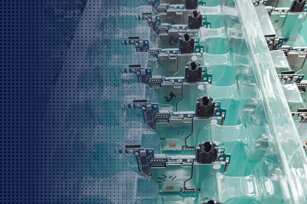
A printed circuit board is a layer of fibreglass with copper traces etched into it. On its own, it does nothing. PCB Assembly – PCBA – is the process of populating that board with electronic components and soldering them into place to create a functioning electronic circuit. It is the manufacturing step that turns a design into a working device.
PCB vs. PCBA: Understanding the Difference
A PCB (Printed Circuit Board) is the bare board – the substrate with copper tracks, pads, and vias that defines how components will connect electrically.
A PCBA (Printed Circuit Board Assembly) is the PCB with all electronic components – resistors, capacitors, ICs, connectors – mounted and soldered in their correct positions. It is the working unit ready for integration into a final product.
When you send a design to an EMS provider, you send Gerber files and a BOM. They send back a PCBA.
The PCB Assembly Process: 8 Steps Explained
Step 1 – Design Review and Design for Manufacturability (DfM)
Before assembly begins, the EMS provider reviews your Gerber files and BOM for manufacturability. DfM catches issues that would cause defects in production: component pads too close together, insufficient clearance for soldering, components that are difficult to source, or thermal management problems. Fixing these at DfM costs nothing. Fixing them after tooling is expensive.
Step 2 – BOM, Gerber Files, and Pick-and-Place File Preparation
The EMS provider needs four documents to begin assembly:
- Gerber files: The PCB layout in machine-readable format
- Bill of Materials (BOM): Every component, its part number, manufacturer, and quantity
- Pick-and-Place file (CPL): X-Y coordinates and rotation for every component placement
- NC Drill file: Hole locations and sizes for drilling and via formation
Step 3 – Solder Paste Application via Stencil
A laser-cut stainless steel stencil – precisely aperture-matched to your PCB’s solder pad pattern – is aligned over the board. Solder paste (a mixture of flux and fine tin-silver-copper particles) is spread across the stencil with a squeegee, depositing controlled volumes of paste exactly where components will be placed. Solder paste inspection (SPI) follows to verify paste volume and alignment before placement.
Step 4 – Component Placement (SMT Pick-and-Place)
High-speed pick-and-place machines read the CPL file and precisely place surface mount components onto the paste-covered pads. Modern machines place upwards of 30,000 components per hour. For fine-pitch and ultra-miniature components (0201, 01005), precision optical alignment systems verify placement accuracy in real time.
Step 5 – Reflow Soldering
The populated board passes through a reflow oven – a conveyor furnace with a precisely controlled temperature profile. The solder paste melts, wets the component leads and PCB pads, and solidifies on cooling to form permanent electrical joints. The reflow profile (preheat, soak, reflow, cool-down) is designed for the specific solder alloy and component thermal requirements.
Step 6 – Through-Hole Component Insertion and Wave Soldering
Not all components are surface mount. Connectors, large capacitors, transformers, and components requiring mechanical strength are inserted through holes in the PCB and soldered by wave soldering – passing the underside of the board over a wave of molten solder that forms joints at every exposed through-hole lead simultaneously.
For low-volume or mixed assemblies, selective soldering or hand soldering by certified operators (to IPC-A-610 workmanship standards) is used instead of wave soldering.
Step 7 – Automated Optical Inspection (AOI)
Every assembled board passes through an AOI machine – a high-resolution camera system that scans the board and compares every component placement, solder joint, and orientation against the approved reference image. Missing components, tombstoning, solder bridges, and polarity reversals are flagged. AOI catches visible defects with high throughput and consistency.
X-ray inspection is added for BGA (Ball Grid Array) components, where solder joints are hidden under the package and invisible to AOI.
Step 8 – In-Circuit Testing (ICT) and Functional Testing
In-Circuit Testing uses a bed-of-nails fixture or flying probe system to verify electrical connectivity, component values, and circuit functionality – catching shorts, opens, wrong values, and missing components that assembly inspection might miss.
Functional Testing simulates the board’s operation in its intended application. The test fixture applies power, stimulus signals, and loads, and verifies the board performs to its functional specification. For complex products, this is the ultimate quality gate.
SMT vs. Through-Hole vs. Mixed Technology
| Technology | Best For | Key Advantage | Key Limitation |
|---|---|---|---|
| SMT | Consumer electronics, IoT, wearables | Speed, density, cost at volume | Less mechanical strength at joints |
| Through-hole | Connectors, power components, aerospace/mil | Mechanical strength, proven reliability | Larger board area, slower |
| Mixed | Complex boards with both requirements | Flexibility | Higher process complexity |
Quality Standards: What IPC-A-610 Means for Your PCB
IPC-A-610 (Acceptability of Electronic Assemblies) is the globally recognised standard that defines what a good solder joint, component placement, and assembly looks like – and what is rejectable. Every EMS provider worth working with trains and certifies their operators and inspectors to IPC-A-610.
When specifying a PCBA order, indicate the required IPC-A-610 Class:
- Class 1: General electronics – consumer products with minimal performance requirements
- Class 2: Dedicated service electronics – most industrial and commercial products
- Class 3: High-performance electronics – aerospace, defence, medical, and life-critical products
From Prototype to Mass Production
NPI and First Article Inspection
New Product Introduction (NPI) is the structured process of taking a design from prototype to production-qualified. It includes engineering validation builds (EVT), design validation builds (DVT), and production validation builds (PVT), each at increasing volume and process rigour.
First Article Inspection is the formal dimensional and functional verification of the first production article – documented evidence that the EMS process produces a board that conforms to the design intent before volume production is released.
Engineering Validation Testing (EVT, DVT, PVT)
- EVT: Does the electronic design work as intended?
- DVT: Does it survive environmental stress – temperature, humidity, vibration?
- PVT: Can it be produced consistently at volume with acceptable yield?
Skipping or compressing NPI stages is the most common root cause of quality escapes in electronics manufacturing.
Scaling to High-Volume Production Runs
High-volume production requires dedicated SMT line programming, approved production control plans, statistical process control (SPC) on critical process parameters, and regular measurement system analysis (MSA) for test fixtures. These investments are made during NPI and sustained through production life.
Component Sourcing and Supply Chain Integration
BOM Management and Approved Vendor Lists
A PCBA is only as good as its components. EMS providers maintain Approved Vendor Lists (AVLs) – qualified sources for each BOM item – and manage procurement from authorised distributors (franchised or authorised distribution chain) to eliminate counterfeit component risk.
Component Shortage Risk and Mitigation
The semiconductor shortage of 2020–2022 demonstrated the supply chain vulnerability of electronics manufacturing. Mitigation strategies include:
- Long-lead-time component pre-booking
- Approved alternate sources maintained on the AVL
- Vendor-Managed Inventory (VMI) buffer for critical components
- Last-time-buy planning for end-of-life components
VMI and Consignment Models
In VMI, the EMS provider holds safety stock of OEM-specified components, replenishing against the OEM’s demand signal. In a consignment model, the OEM pre-purchases and ships components to the EMS facility. Both models reduce production lead time and protect against external supply disruption.
How to Select a PCB Assembly Partner
Key Certifications
- ISO 9001: QMS baseline
- IPC-A-610 / J-STD-001: Electronics assembly workmanship
- IATF 16949: Required for automotive PCBA
- AS9100: Required for aerospace/defence PCBA
- ISO 13485: Required for medical device PCBA
Questions to Ask Your EMS Provider
- What component size range can your SMT lines handle?
- What is your first-pass yield rate for comparable assemblies?
- How do you manage AVL and counterfeit component risk?
- What test coverage do you offer (AOI, X-ray, ICT, functional)?
- Can you support NPI through to volume ramp on a single platform?
Prototyping Turnaround Time Benchmarks
- Bare PCB fabrication: 3–5 days (expedite), 7–10 days (standard)
- PCBA prototype build: 5–10 days from approved files
- NPI first article: 2–4 weeks including DfM review
Key Takeaways
- PCBA is the process of mounting and soldering electronic components onto a PCB to create a working assembly
- The 8-step process runs from DfM review through functional testing
- IPC-A-610 Class defines the workmanship standard – Class 3 for aerospace/defence/medical, Class 2 for most commercial products
- Component sourcing, AVL management, and shortage risk mitigation are as important as the assembly process itself
- Selecting a certified EMS partner with full NPI capability is the difference between a smooth launch and an expensive rework cycle
FAQ
Q. What files do I need to provide for PCB assembly?
Gerber files (PCB layout), BOM (component list), Pick-and-Place file (component locations and orientations), and NC Drill file (hole data).
Q. What is the difference between SMT and through-hole PCB assembly?
SMT mounts components on the surface of the PCB and uses reflow soldering – faster, cheaper, and allows higher component density. Through-hole inserts component leads through holes in the PCB and uses wave or selective soldering – provides higher mechanical strength.
Q. What does IPC-A-610 Class 3 mean?
IPC-A-610 Class 3 is the highest workmanship standard, required for electronics where failure is not acceptable – aerospace, defence, medical. It requires the tightest inspection criteria and zero-defect tolerance on critical parameters.