SMT vs. Through-Hole Assembly: Which PCB Technology Is Right for Your Product?

Every PCB carries a fundamental design decision: should your components be surface-mounted, inserted through holes, or a mix of both? The answer shapes your board’s size, cost, reliability, and the EMS capabilities you need to produce it. This guide gives you a rigorous comparison and a clear decision framework.

The Two Fundamental PCB Assembly Methods

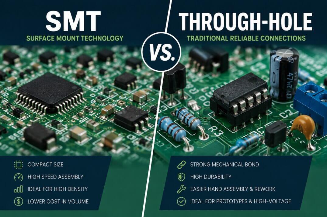
Surface Mount Technology (SMT): How It Works

In SMT, components are placed directly on the surface of the PCB on pre-tinned pads. Solder paste is printed onto the pads, components are placed by automated pick-and-place machines, and the entire board is passed through a reflow oven where the solder paste melts and solidifies to form permanent joints.

SMT components do not penetrate the board. They sit on it.

Through-Hole Technology (THT): How It Works

In THT, components have wire leads that are inserted through drilled holes in the PCB and soldered on the underside – either by wave soldering (for volume) or by hand (for low-volume or complex assemblies). The mechanical engagement of lead-through-hole provides a significantly stronger joint than the surface-to-pad contact of SMT.

The Historical Shift from THT to SMT

Through-hole technology dominated PCB assembly from the 1950s through the 1980s. Surface mount technology emerged in the 1970s and became the dominant method for commercial electronics by the 1990s, driven by the demand for miniaturisation and automation. Today, SMT accounts for the overwhelming majority of commercial electronics assembly volume – but through-hole has never gone away, and for good reason.

Head-to-Head Comparison Across 7 Dimensions

Cost and Throughput

SMT wins comprehensively on cost and speed at volume. Automated pick-and-place machines place 20,000–50,000 components per hour. Wave soldering processes an entire board’s through-hole joints in seconds. But the tooling requirement – solder stencil, pick-and-place programming, reflow profile development – means SMT’s cost advantage is most pronounced at mid-to-high volumes.

Through-hole assembly is more labour-intensive: insertion is typically manual, and hand soldering adds time. At low volumes, the labour cost delta is manageable; at high volumes, it becomes a significant cost driver.

SMT advantage at volume. THT competitive at very low volume with simple designs.

Board Size and Component Density

SMT components are dramatically smaller than their through-hole equivalents. A surface-mount 0402 resistor (1mm × 0.5mm) delivers the same electrical function as a through-hole resistor that is 20× larger. SMT boards can be two to four times denser than equivalent through-hole boards – enabling the miniaturised products that define modern consumer electronics.

SMT: clear winner for size and density.

Mechanical Strength and Vibration Resistance

Through-hole joints are mechanically superior. The lead passes through the board and is soldered to a pad on the opposite side – creating a joint that is anchored in three dimensions. Through-hole joints can withstand forces up to 10× greater than equivalent SMT joints.

In applications subject to mechanical shock, vibration, thermal cycling, or physical stress – connectors, power inductors, military electronics, automotive underbonnet – through-hole provides reliability that SMT cannot match.

THT: clear winner for mechanical strength.

Design Flexibility and Complexity

SMT enables designs that are simply impossible with through-hole: fine-pitch ICs with 0.4mm lead spacing, BGA packages with hundreds of solder balls under the package, micro-connectors. Modern electronic products cannot be designed without SMT.

Through-hole has geometrical constraints: you need a drilled hole for every lead, which limits board routing flexibility and increases board thickness requirements.

SMT: clear winner for design flexibility.

Prototyping Speed

Through-hole components can be inserted and soldered by hand without stencils or programming. This makes through-hole faster for one-off prototypes and proof-of-concept builds where no tooling exists.

SMT prototypes require stencil fabrication (fast – 24–48 hours) and pick-and-place programming, but can also be manually placed for very small quantities.

THT: marginal advantage for hand-build prototypes. Neutral for tooled prototyping.

Repairability and Rework

Through-hole components can be desoldered and replaced with basic soldering equipment. SMT rework requires hot-air rework stations, vacuum pickup tools, and operator skill – particularly for BGA and other hidden-joint packages.

THT: advantage for field repair and rework. SMT requires specialised tools.

High-Frequency and RF Performance

SMT components have shorter lead lengths than through-hole equivalents – which means lower parasitic inductance and capacitance. At frequencies above ~100MHz, this becomes increasingly significant: through-hole leads act as antennas and degrade signal integrity. RF designs, high-speed digital circuits, and microwave applications almost always specify SMT or embedded components.

SMT: clear winner for high-frequency performance.

Industries and Applications: When Each Technology Dominates

SMT: Consumer Electronics, IoT, Wearables, Automotive

Smartphones, tablets, laptops, smartwatches, earbuds, IoT sensors, automotive ECUs – every one of these is built with SMT as the primary technology. The combination of miniaturisation, throughput, and high-frequency performance that SMT enables is non-negotiable for these applications.

Through-Hole: Aerospace, Military, Power Supplies, Connectors

Mains connectors, high-voltage capacitors, power inductors, terminal blocks, and any component that will experience mechanical stress or vibration uses through-hole. In aerospace and military applications, connector integrity under shock and vibration is a life-safety issue – through-hole is specified by standards. Power supply designs use through-hole for heat-generating components where the board provides a mechanical anchor and thermal mass.

Mixed Technology Boards: Getting the Best of Both

Most real-world PCBs use both technologies. A consumer product might use SMT for all ICs, passives, and RF components while using through-hole for its USB connector, its large electrolytic capacitors, and its mechanical mounting points.

Design Considerations for Mixed Assemblies

Mixed technology adds design complexity: the solder process sequence matters. Typically:

  1. SMT bottom side → reflow
  2. SMT top side → reflow
  3. Through-hole insertion → wave or selective soldering

Components that cannot survive wave soldering (many SMT components on the bottom side) must be masked or hand-soldered. This adds process steps and cost.

Manufacturing Sequence for Mixed Boards

Mixed assembly requires coordination between SMT lines, through-hole insertion, and soldering operations – including managing thermal sensitivity across the same board. An EMS provider with mixed-technology capability handles this sequencing as standard; inexperienced assemblers will struggle.

Cost Premium of Mixed Technology

Mixed technology adds approximately 15–25% to assembly cost versus pure SMT, due to the additional process steps, masking, and through-hole labour. For most designs, this premium is warranted by the functional requirements.

The Decision Framework: 5 Questions to Determine Your Choice

  1. Is miniaturisation critical? If yes → SMT required.
  2. Will the product experience mechanical shock or vibration? If yes → specify through-hole for mechanically critical components.
  3. Does your design include RF or high-frequency circuitry? If yes → SMT required for RF components.
  4. Will the product be field-repaired? If yes → consider through-hole for connectors and serviceable components.
  5. What is your production volume? High volume → SMT economics dominate. Very low volume, simple design → through-hole hand assembly may be sufficient.

For most commercial electronics products, the answer is mixed technology – SMT for electronics functions, through-hole for mechanical interfaces.

Choosing an EMS Partner for Your Technology Type

SMT Line Capabilities to Look For

  • Component placement range (minimum size: can they handle 0201 or 01005?)
  • Placement accuracy (±0.05mm is standard; ±0.025mm for fine-pitch)
  • X-ray inspection capability (essential for BGA)
  • Reflow oven profile control (critical for lead-free and thermal-sensitive components)

Through-Hole and Hand-Soldering Expertise

  • IPC-A-610 certified operators for hand soldering
  • Wave soldering with selective masking capability
  • Selective soldering machines for complex mixed boards

Mixed Technology Assembly Competency

Ask specifically for mixed-technology reference boards – proof that the EMS provider has managed the SMT/THT sequence on comparable assemblies. This is not universal capability.

India EMS: Cost Implications by Assembly Type

SMT Cost per PCB in India vs. China

India’s labour cost advantage is most visible in labour-intensive SMT operations – specifically in:

  • High-mix, low-volume boards where set-up and changeover dominate
  • Through-hole and hand-assembly content within mixed boards
  • Inspection and test operations

For high-volume, fully automated SMT, the labour cost delta narrows – but India’s PLI incentives and lower overhead costs maintain a meaningful advantage.

Labour-Intensive Through-Hole: Where India Has an Edge

Through-hole insertion, selective soldering, and final assembly operations that rely on skilled manual labour are where India’s labour cost advantage is most pronounced relative to China. For products with significant through-hole content – industrial controls, power electronics, defence systems – India EMS providers offer a compelling total cost advantage.

Key Takeaways

  • SMT dominates for miniaturisation, throughput, cost at volume, and high-frequency performance
  • Through-hole dominates for mechanical strength, repairability, and high-power components
  • Most commercial electronics use mixed technology – SMT for electronics functions, through-hole for mechanical interfaces
  • The 5-question framework guides technology selection: miniaturisation, vibration, RF, repairability, and volume
  • India EMS providers are particularly competitive for mixed-technology and through-hole-heavy assemblies where labour intensity is high

FAQ

Can I use both SMT and through-hole on the same PCB?
Yes – this is called mixed technology assembly and is the norm for most commercial electronics. Your EMS provider manages the two-stage assembly process.

Which technology is better for aerospace and defence?
Both are used. SMT is used for electronics density and performance. Through-hole is specified for mechanical interfaces and safety-critical connections. AS9100-certified EMS providers are qualified for both.

Does SMT cost less than through-hole?
At volume, yes – automated SMT is faster and less labour-intensive than through-hole insertion. At very low volumes with simple designs, through-hole hand assembly can be comparable. Mixed technology is typically 15–25% more expensive than pure SMT.

What Is PCB Assembly? A Complete Step-by-Step Guide (PCBA Explained)

A printed circuit board is a layer of fibreglass with copper traces etched into it. On its own, it does nothing. PCB Assembly – PCBA – is the process of populating that board with electronic components and soldering them into place to create a functioning electronic circuit. It is the manufacturing step that turns a design into a working device.

PCB vs. PCBA: Understanding the Difference

PCB (Printed Circuit Board) is the bare board – the substrate with copper tracks, pads, and vias that defines how components will connect electrically.

PCBA (Printed Circuit Board Assembly) is the PCB with all electronic components – resistors, capacitors, ICs, connectors – mounted and soldered in their correct positions. It is the working unit ready for integration into a final product.

When you send a design to an EMS provider, you send Gerber files and a BOM. They send back a PCBA.

The PCB Assembly Process: 8 Steps Explained

Step 1 – Design Review and Design for Manufacturability (DfM)

Before assembly begins, the EMS provider reviews your Gerber files and BOM for manufacturability. DfM catches issues that would cause defects in production: component pads too close together, insufficient clearance for soldering, components that are difficult to source, or thermal management problems. Fixing these at DfM costs nothing. Fixing them after tooling is expensive.

Step 2 – BOM, Gerber Files, and Pick-and-Place File Preparation

The EMS provider needs four documents to begin assembly:

  • Gerber files: The PCB layout in machine-readable format
  • Bill of Materials (BOM): Every component, its part number, manufacturer, and quantity
  • Pick-and-Place file (CPL): X-Y coordinates and rotation for every component placement
  • NC Drill file: Hole locations and sizes for drilling and via formation

Step 3 – Solder Paste Application via Stencil

A laser-cut stainless steel stencil – precisely aperture-matched to your PCB’s solder pad pattern – is aligned over the board. Solder paste (a mixture of flux and fine tin-silver-copper particles) is spread across the stencil with a squeegee, depositing controlled volumes of paste exactly where components will be placed. Solder paste inspection (SPI) follows to verify paste volume and alignment before placement.

Step 4 – Component Placement (SMT Pick-and-Place)

High-speed pick-and-place machines read the CPL file and precisely place surface mount components onto the paste-covered pads. Modern machines place upwards of 30,000 components per hour. For fine-pitch and ultra-miniature components (0201, 01005), precision optical alignment systems verify placement accuracy in real time.

Step 5 – Reflow Soldering

The populated board passes through a reflow oven – a conveyor furnace with a precisely controlled temperature profile. The solder paste melts, wets the component leads and PCB pads, and solidifies on cooling to form permanent electrical joints. The reflow profile (preheat, soak, reflow, cool-down) is designed for the specific solder alloy and component thermal requirements.

Step 6 – Through-Hole Component Insertion and Wave Soldering

Not all components are surface mount. Connectors, large capacitors, transformers, and components requiring mechanical strength are inserted through holes in the PCB and soldered by wave soldering – passing the underside of the board over a wave of molten solder that forms joints at every exposed through-hole lead simultaneously.

For low-volume or mixed assemblies, selective soldering or hand soldering by certified operators (to IPC-A-610 workmanship standards) is used instead of wave soldering.

Step 7 – Automated Optical Inspection (AOI)

Every assembled board passes through an AOI machine – a high-resolution camera system that scans the board and compares every component placement, solder joint, and orientation against the approved reference image. Missing components, tombstoning, solder bridges, and polarity reversals are flagged. AOI catches visible defects with high throughput and consistency.

X-ray inspection is added for BGA (Ball Grid Array) components, where solder joints are hidden under the package and invisible to AOI.

Step 8 – In-Circuit Testing (ICT) and Functional Testing

In-Circuit Testing uses a bed-of-nails fixture or flying probe system to verify electrical connectivity, component values, and circuit functionality – catching shorts, opens, wrong values, and missing components that assembly inspection might miss.

Functional Testing simulates the board’s operation in its intended application. The test fixture applies power, stimulus signals, and loads, and verifies the board performs to its functional specification. For complex products, this is the ultimate quality gate.

SMT vs. Through-Hole vs. Mixed Technology

TechnologyBest ForKey AdvantageKey Limitation
SMTConsumer electronics, IoT, wearablesSpeed, density, cost at volumeLess mechanical strength at joints
Through-holeConnectors, power components, aerospace/milMechanical strength, proven reliabilityLarger board area, slower
MixedComplex boards with both requirementsFlexibilityHigher process complexity

Quality Standards: What IPC-A-610 Means for Your PCB

IPC-A-610 (Acceptability of Electronic Assemblies) is the globally recognised standard that defines what a good solder joint, component placement, and assembly looks like – and what is rejectable. Every EMS provider worth working with trains and certifies their operators and inspectors to IPC-A-610.

When specifying a PCBA order, indicate the required IPC-A-610 Class:

  • Class 1: General electronics – consumer products with minimal performance requirements
  • Class 2: Dedicated service electronics – most industrial and commercial products
  • Class 3: High-performance electronics – aerospace, defence, medical, and life-critical products

From Prototype to Mass Production

NPI and First Article Inspection

New Product Introduction (NPI) is the structured process of taking a design from prototype to production-qualified. It includes engineering validation builds (EVT), design validation builds (DVT), and production validation builds (PVT), each at increasing volume and process rigour.

First Article Inspection is the formal dimensional and functional verification of the first production article – documented evidence that the EMS process produces a board that conforms to the design intent before volume production is released.

Engineering Validation Testing (EVT, DVT, PVT)

  • EVT: Does the electronic design work as intended?
  • DVT: Does it survive environmental stress – temperature, humidity, vibration?
  • PVT: Can it be produced consistently at volume with acceptable yield?

Skipping or compressing NPI stages is the most common root cause of quality escapes in electronics manufacturing.

Scaling to High-Volume Production Runs

High-volume production requires dedicated SMT line programming, approved production control plans, statistical process control (SPC) on critical process parameters, and regular measurement system analysis (MSA) for test fixtures. These investments are made during NPI and sustained through production life.

Component Sourcing and Supply Chain Integration

BOM Management and Approved Vendor Lists

A PCBA is only as good as its components. EMS providers maintain Approved Vendor Lists (AVLs) – qualified sources for each BOM item – and manage procurement from authorised distributors (franchised or authorised distribution chain) to eliminate counterfeit component risk.

Component Shortage Risk and Mitigation

The semiconductor shortage of 2020–2022 demonstrated the supply chain vulnerability of electronics manufacturing. Mitigation strategies include:

  • Long-lead-time component pre-booking
  • Approved alternate sources maintained on the AVL
  • Vendor-Managed Inventory (VMI) buffer for critical components
  • Last-time-buy planning for end-of-life components

VMI and Consignment Models

In VMI, the EMS provider holds safety stock of OEM-specified components, replenishing against the OEM’s demand signal. In a consignment model, the OEM pre-purchases and ships components to the EMS facility. Both models reduce production lead time and protect against external supply disruption.

How to Select a PCB Assembly Partner

Key Certifications

  • ISO 9001: QMS baseline
  • IPC-A-610 / J-STD-001: Electronics assembly workmanship
  • IATF 16949: Required for automotive PCBA
  • AS9100: Required for aerospace/defence PCBA
  • ISO 13485: Required for medical device PCBA

Questions to Ask Your EMS Provider

  • What component size range can your SMT lines handle?
  • What is your first-pass yield rate for comparable assemblies?
  • How do you manage AVL and counterfeit component risk?
  • What test coverage do you offer (AOI, X-ray, ICT, functional)?
  • Can you support NPI through to volume ramp on a single platform?

Prototyping Turnaround Time Benchmarks

  • Bare PCB fabrication: 3–5 days (expedite), 7–10 days (standard)
  • PCBA prototype build: 5–10 days from approved files
  • NPI first article: 2–4 weeks including DfM review

Key Takeaways

  • PCBA is the process of mounting and soldering electronic components onto a PCB to create a working assembly
  • The 8-step process runs from DfM review through functional testing
  • IPC-A-610 Class defines the workmanship standard – Class 3 for aerospace/defence/medical, Class 2 for most commercial products
  • Component sourcing, AVL management, and shortage risk mitigation are as important as the assembly process itself
  • Selecting a certified EMS partner with full NPI capability is the difference between a smooth launch and an expensive rework cycle

FAQ

What files do I need to provide for PCB assembly?
Gerber files (PCB layout), BOM (component list), Pick-and-Place file (component locations and orientations), and NC Drill file (hole data).

What is the difference between SMT and through-hole PCB assembly?
SMT mounts components on the surface of the PCB and uses reflow soldering – faster, cheaper, and allows higher component density. Through-hole inserts component leads through holes in the PCB and uses wave or selective soldering – provides higher mechanical strength.

What does IPC-A-610 Class 3 mean?
IPC-A-610 Class 3 is the highest workmanship standard, required for electronics where failure is not acceptable – aerospace, defence, medical. It requires the tightest inspection criteria and zero-defect tolerance on critical parameters.

Electronics Manufacturing Services (EMS) in India: The Complete 2026 Guide

India assembled its first iPhone in 2017. By 2025, Apple’s Indian production crossed INR 2 trillion – an 85% jump in a single year – representing roughly 25% of global iPhone output. What happened in those eight years is one of the most consequential industrial stories of the decade: India became a credible, large-scale electronics manufacturing destination, and the EMS ecosystem that built up around that transformation is now available to any OEM in the world.

This guide covers what Electronics Manufacturing Services providers in India actually offer, why India’s cost and policy environment makes it compelling, what the EMS market looks like, which industries are being served, and how to choose a partner.

What Are Electronics Manufacturing Services?

EMS refers to the design, manufacture, testing, and logistics services that contract manufacturers provide to electronics OEMs who outsource production. An EMS provider does not own the product design – that belongs to the OEM. They own the process expertise, equipment, supply chain relationships, and facilities that turn the OEM’s design into a shipping product.

EMS vs. OEM vs. ODM: Key Differences

  • EMS provider: Builds to the OEM’s design. No product ownership.
  • OEM (Original Equipment Manufacturer): Designs and brands the product; may manufacture or outsource production.
  • ODM (Original Design Manufacturer): Designs the product and manufactures it; OEM buys finished product, often white-labelled.

Zetwerk and the EMS providers in its network operate on the EMS model – building to client specifications with no claim on product design or IP.

The Full Scope of EMS: Design Through Distribution

Modern EMS is not just assembly. Full-service EMS providers support the complete product lifecycle:

  • Design support: DfM review, PCB layout advisory, component selection optimisation
  • Prototyping and NPI: New Product Introduction, engineering validation builds
  • PCB assembly: SMT and through-hole, AOI, X-ray, ICT
  • Box build and system integration: Mechanical assembly, cable harness, final product integration
  • Testing: Functional test, environmental stress screening, burn-in
  • Component sourcing: Global BOM procurement, approved vendor list management
  • Distribution: Warehousing, VMI, JIT delivery, repair and refurbishment

What EMS Companies in India Actually Provide

PCB Assembly (SMT and Through-Hole)

India’s EMS sector has invested heavily in surface mount technology lines – automated pick-and-place, solder paste inspection, reflow ovens, and automated optical inspection. SMT is the dominant technology for consumer electronics, wearables, and industrial electronics. Through-hole capability is maintained for connectors, power components, and applications requiring mechanical strength.

Box Build and System Integration

Beyond the PCB, box build encompasses mechanical assembly, cable harness integration, sub-assembly mating, and final product build. India’s EMS providers combine electronics assembly with mechanical fabrication capability – including sheet metal, die casting, and plastics – to deliver fully integrated products.

Component Sourcing and BOM Management

Component sourcing is a strategic capability. India’s EMS providers maintain global supply chain relationships – with distributors and manufacturers in Asia, Europe, and North America – to procure to approved vendor lists, manage component obsolescence, and mitigate shortage risk. Vendor-managed inventory (VMI) and just-in-time delivery reduce the OEM’s working capital requirements.

Testing: ICT, Functional, Environmental

Production testing in Indian EMS follows IPC standards:

  • In-Circuit Testing (ICT): Electrical connectivity, component values, and shorts
  • Functional Testing: Full product operation under simulated end-use conditions
  • Automated Optical Inspection (AOI) and X-ray: Solder joint quality and hidden defect detection
  • Environmental Stress Screening: Temperature cycling, vibration, humidity – required for automotive and industrial products

Repair and After-Sales Services

Leading Indian EMS providers offer repair depots and refurbishment services for warranty and post-warranty returns – extending the EMS relationship from build to product lifecycle management.

Why India Is Winning in Electronics Manufacturing

Labour Cost Advantage Over China

India’s EMS labour costs average USD 3/hour compared to China’s USD 5.80/hour. For labour-intensive assembly operations – wearables, hearables, industrial products with high touch-content – this delta is significant at volume.

Engineering Talent Pool: 1.5M+ STEM Graduates Per Year

India’s engineering talent pipeline is one of the world’s deepest. Electronics engineering, embedded systems, and test engineering talent is available in large volumes in Chennai, Hyderabad, Bangalore, and Pune – the same cities with strong EMS infrastructure. This technical talent base supports DfM, NPI, and test development work that many EMS providers in other low-cost geographies cannot match.

PLI Scheme: 4-6% Incentive on Incremental Production

India’s Production Linked Incentive scheme for Large Scale Electronics Manufacturing provides a 4–6% financial incentive on incremental production above a base year threshold. This incentive has driven Foxconn, Pegatron, Rising Star (iPhone supply chain), Lava, Dixon, and others to invest in India EMS capacity. It translates to a meaningful pricing advantage for OEMs sourcing from PLI-registered EMS providers.

ECMS 2025: India’s ₹22,919 Cr Component Manufacturing Push

The Electronics Component Manufacturing Scheme approved in 2025 specifically targets the component gap in India’s EMS ecosystem – PCBs, SMD passives, lithium-ion cells, and other foundational components. This policy signals a deliberate effort to build component depth that will further reduce India’s EMS cost structure over the next 5 years.

India’s EMS Market: Size, Growth, and Key Players

Market Overview

India’s electronics production grew from ₹1.9 lakh crore in 2014–15 to ₹11.3 lakh crore in 2024–25 – a six-fold increase over ten years. Electronics exports rose from ₹38,000 crore to ₹3.27 lakh crore in the same period. The EMS sector is at the centre of this growth.

The India EMS market is growing at a CAGR above 20%, driven by mobile phones, wearables, IT hardware, and automotive electronics.

Key Capability Categories

India’s EMS ecosystem covers:

  • High-volume consumer electronics: Mobile phones, tablets, laptops, earbuds, smartwatches
  • Industrial and B2B electronics: Smart meters, inverters, industrial controls, telecom equipment
  • Automotive electronics: EV charging controllers, ADAS sensors, infotainment systems
  • Aerospace and defence electronics: Avionics, radar sub-systems, defence communications equipment

Industries Driving EMS Demand in India

Consumer Electronics (Smartphones, Laptops, Wearables)

Mobile phones account for the largest share of India’s EMS output. Laptop and IT hardware manufacturing is growing rapidly under PLI. Wearables – smartwatches, earbuds, fitness bands – are an emerging high-growth segment with strong domestic demand.

Automotive and EV Electronics

As India’s automotive sector transitions to electric vehicles, the demand for EV power electronics, battery management systems, charging infrastructure, and ADAS components is growing significantly. India’s automotive electronics EMS market is projected to grow at above 25% annually through 2030.

Telecom and Networking Equipment

India’s 5G rollout is driving demand for telecom equipment manufacturing. India has set explicit domestic manufacturing content requirements for government telecom procurement – a structural demand driver for domestic EMS.

Aerospace and Defence Electronics

India’s private aerospace and defence manufacturing sector is growing rapidly under liberalised FDI rules and indigenisation targets. Avionics assemblies, defence communication systems, and radar sub-systems are being manufactured by Indian EMS companies with AS9100 and NADCAP certification.

Industrial Controls and Smart Meters

India’s smart grid rollout and industrial automation adoption are driving demand for smart meters, SCADA controllers, and industrial IoT devices – all manufactured through EMS.

EMS for Wearables and Hearables: India’s Emerging Edge

The wearables and hearables market is one of the fastest-growing segments of consumer electronics globally – and one where India has built genuine EMS capability.

Smartwatch and Earbuds Manufacturing Landscape

Brands like boAt, Noise, and Boat have built global-scale wearables brands manufactured entirely in India. The EMS ecosystem supporting them – PCB assembly for miniaturised boards, precision die casting for chassis, injection moulding for housings, battery integration, and functional testing – is now available to global OEMs looking to produce wearables in India.

IoT Devices and Smart Home Products

The IoT product category – smart home devices, connected sensors, edge computing hardware – requires EMS capability in small-form-factor PCB assembly, wireless module integration (Wi-Fi, Bluetooth, Zigbee), and firmware flashing. Indian EMS providers are increasingly competent in this category.

Key Capabilities Required for Wearable EMS

  • Ultra-miniature SMT (0201 and 01005 component capability)
  • Flexible PCB assembly
  • Battery integration and safety testing
  • Waterproofing and IP rating processes
  • Cosmetic-grade mechanical finishing

Full Product Lifecycle Manufacturing – The Platform Model

From Concept to Prototype: Design for Manufacturability

Before a single unit is assembled, DfM review identifies design choices that will drive cost, quality risk, or supply chain complexity. Fixing a component selection or PCB layout at DfM stage costs a fraction of what it costs to fix in production.

NPI: New Product Introduction and First Article Inspection

NPI is the structured process of moving from approved design to qualified production. In India’s EMS ecosystem, NPI includes engineering validation builds (EVT), design validation builds (DVT), production validation builds (PVT), and First Article Inspection – each stage adding production confidence before volume ramp.

Mass Production, VMI, and JIT Delivery

At production scale, India’s EMS providers offer vendor-managed inventory programmes – where the EMS provider holds safety stock of critical components – and just-in-time delivery to the OEM’s demand signal. Zetwerk’s platform delivers JIT lead times as fast as five days for pre-stocked materials.

After-Sales Repair and Refurbishment

A full-service EMS partnership extends to after-sales: warranty repair, component-level rework, refurbishment for return-to-market, and end-of-life processing. This keeps the EMS partner engaged through the full product lifecycle rather than just the manufacturing phase.

EMS Cost Breakdown: India vs. China vs. Vietnam

Cost ComponentIndiaChinaVietnam
Labour (assembly)LowMediumLow
Engineering talentHigh availability, competitive costHigh availability, higher costLimited availability
PLI subsidy4–6%NoneNone
Component sourcingMostly global/Asian supply chainStrong domestic ecosystemMostly imported
Logistics to US/EUSlightly longerShorterSimilar to India
IP riskManagedHigherManaged
LanguageEnglish strongEnglish limitedEnglish limited

India’s total landed cost advantage over China for EMS work has narrowed as China’s wages have risen – but the PLI subsidy, English proficiency, and geopolitical safety advantage have shifted the calculus meaningfully in India’s favour for a broad range of electronics categories.

How to Choose the Right EMS Partner in India

Certifications to Require

  • ISO 9001 – baseline QMS
  • IPC-A-610 – electronics workmanship
  • J-STD-001 – soldering
  • IATF 16949 – if automotive
  • AS9100 – if aerospace or defence
  • ISO 13485 – if medical devices

8 Evaluation Criteria for EMS Selection

  1. SMT capability: line count, component size range, throughput
  2. Through-hole and mixed-technology capability
  3. Inspection suite: AOI, X-ray, ICT
  4. Component sourcing breadth and BOM management
  5. NPI process rigour and DfM capability
  6. Quality certifications and audit records
  7. Capacity and lead time track record
  8. Digital visibility and reporting tools

Questions to Ask During RFQ

  • What is your SMT component placement accuracy and yield rate?
  • What is your average BOM lead time from RFQ to first article?
  • Can you demonstrate NPI builds for products of similar complexity?
  • How do you manage component shortage risk?
  • What is your repair/rework rate in production?

Key Takeaways

  • India’s EMS market is growing above 20% annually – driven by PLI incentives, rising global EMS demand, and a deepening capability ecosystem
  • Core EMS services span PCB assembly, box build, component sourcing, testing, and distribution
  • Labour cost, STEM talent, PLI incentives, and IP law alignment give India structural EMS advantages
  • Wearables, automotive electronics, telecom, and defence are the highest-growth EMS segments
  • Full product lifecycle EMS – design support through repair – is available from India’s leading providers
  • Platform-based EMS (Zetwerk) provides pre-vetted access to this ecosystem with production visibility and accountability

FAQs

What types of products can India’s EMS providers manufacture?
Consumer electronics, industrial controls, automotive electronics, defence/aerospace systems, medical devices, telecom equipment, wearables, IoT devices, and IT hardware – the full range of electronics product categories.

How does the PLI scheme benefit OEMs sourcing EMS from India?
PLI provides Indian EMS companies a 4–6% financial incentive on incremental production, which is partially reflected in competitive pricing. For significant programmes, an OEM can structure production with a PLI-registered EMS provider to capture meaningful cost advantages.

What is the typical lead time for PCB assembly in India?
Prototypes and NPI builds: 2–4 weeks. Production runs: 4–8 weeks from PO, depending on component lead times. Pre-stocked materials on platforms like Zetwerk can deliver JIT in 5 days.